3-Way
Active Loudspeaker |

|
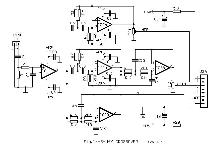
After the 2-way active loudspeaker circuit,
give a complete electronic section circuit of one 3-way active loudspeaker. The
speaker�s choice will become from you, because the particular circuit has the driving
possibility all almost trade loudspeakers. The choice that made in the crossover stage, is
a 3-way crossover [Butterworth] with cut off -point frequencies 200HZ and 3500HZ, with
slope -12dB/oct. These frequencies can change and adapted in your own speaker�s choice,
using the calculation types of Fig.5. Exist the possibility is used other
circuit crossover, as the circuit of 3-way
active crossover with slope -24dB/oct. The circuit crossover does not exist
above in main PCB, but is contact with this via the plug J2A that is applied above in the
J2B. This can become if in the place of J2A it�s placed a pinhead with 8 pin and PCB
crossover put on above main PCB in form sandwich. It can however be placed in other point
and with a flat cable to transport the signals and the voltages from J2A in the J2B. Power
supply for � 15V of the crossover circuits it�s found in
main PCB. A point that I want to highlight is with regard to various in the calculation
values precision and real values of resistors and capacitors. It�s good, if the
component value does not exist in standard value to select a combination that us will give
value near in theoretical and simultaneously to do the same and in the other loudspeaker,
in order that the divergence is same. In the drawing exist parallel combinations
resistors, and somebody�s from these are not used if they do not need. With the TR1-2 we
adjust the level of high and mid speakers, if it needs.
|
| R1=47Kohms |
R19-20=47ohms |
C17-18=47uF 25V |
| R2=1Kohms |
C1=2.2uF 63V MKT |
TR1-2=47Kohms trimmer |
| R3=4.7Kohms |
C2=220pF |
IC1=TL071 |
| R4-11-13-15-17=NC |
C3-4-11-12=100nF
63V MKT |
IC2-3=TL072-NE5532 |
| R5-6=12Kohms |
C5-6-9-10=10nF
63V MKT |
J1=2pin conn. 2.54mm pin
step |
| R7-8=120Kohms |
C13=6.8nF 63V
MKT |
J2A=8pin conn. 2.54mm pin
step |
| R9-10=220Kohms |
C14=3.3nF 63V
MKT |
or 8 pinhead 2.54mm pin
step* |
| R12-14=10Kohms |
C15=33nF 63V MKT |
|
| R6-18=33Kohms |
C16=18nF 63V MKT |
All Resistors is 1/4W 1% |
|
Typical
specifications |
|
|
Input
sensitivity |
1Vrms |
|
|
Input
impedance |
47K |
|
|
High
Pass filter |
20HZ-:-200HZ |
|
|
Band Pass filter |
200HZ-:-3500HZ |
|
|
Low Pass filter |
3500HZ-:-20KHZ |
|
|
Slope |
-12dB/oct |
|
|
|
|
|
|

|
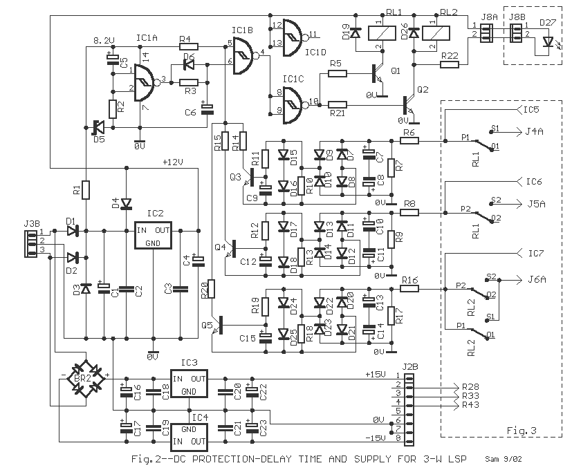
The protection circuit
from DC voltages [Fig.2] and delay connection the speakers is the
same with what exist in 2-way active
loudspeaker where exists and the relative description. They exist certain
various, as has been added a detection stage of continuous voltages and a relay [RL2]. The
contacts of RL1 connect the speakers the high and mid frequencies, the two contacts of RL2
are connected at the parallel and connect the speaker of low frequencies in the exit of
IC7. Here exist also the stage of � 15V supply for the
crossover and suffices for each choice of crossover circuit.
|
| R1=470ohms 1W |
C4=10uF 25V |
IC1=4093 |
| R2-3=1Mohms |
C5=1uF 25V |
IC2=7812 |
| R4=22Kohms |
C6=4.7uF 25V |
IC3=7815 |
| R5-21=33Kohms |
C7-8-10-11-13-14=33uF 63V |
IC4=7915 |
| R6-8-16=15Kohms |
C9-12-15=22uF 16V |
Q1-2=BD678 |
| R7-9-17=56Kohms |
C16-17=2200uF 25V |
Q3-4-5=BC550C |
| R10-23-18=56Kohms |
C22-23=10uF 25V |
RL1-2=12V RELAY G2R2 [OMRON] |
| R11-12-19=10Kohms |
D1-2-3-4=1N4002 |
J2B=8pin conn. 2.54mm pin
step |
| R14-15-20=3.9Kohms |
D5=8.2V 1W Zener |
J3B=3pin conn. 2.54mm pin
step |
| R22=1Kohms |
D6-7.....26=1N4148 |
J8A-B=2pin conn.
2.54mm pin step male-female |
| C1=100uF 25V |
D27=Led 5mm |
| C2-3-18-19-20-21=100nF 63V
MKT |
BR2=BRIDGE RECT. 80V 1.5A |
All Resistors is 1/4W 1-5% |
|

|
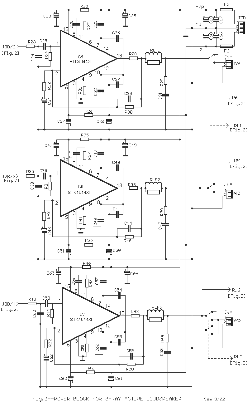
In the Fig.3,
exist the circuit of power amplifiers that drive the corresponding speakers. The choice
are also here the STK4044XI of SANYO with output power roughly 100W each
one, power that consider that is very good for the drive the majority of speakers of
trade, in high levels. The sound quality that produces is very good. The type choice with
clue XI became because it has better and more modern internal designing,
as regards types II and V. It can used also other types [ B and V]
without exists some problem. Filters RLF1�3 are made by a resistor 10R 3W that to around
her we wrap roughly 30 coils in three layer, wire from cupreous insulated with diameter
1mm. The capacitors C66�. 69 are placed above in main PCB and near in the power
amplifiers.
|
| R23-33-43-32-42-52=1Kohms |
RLF1...3=FILTER*
See text |
C32-46-50=1nF 63V MKT |
| R24-34-44=47Kohms |
C24-38-52=330pF |
C33-37-47-51-63-65=100uF 63V |
| R25-26-35-36-45-46=100ohms |
C25-39-26-40-54=1uF
63V MKT |
C34-48-62=220uF 25V |
| R27-37-47=1Kohms |
C53=2.2uF 63V
MKT |
C35-36-49-50-61-64=10uF 63V |
| R28-38-48=0.22ohms 5W |
C27-28-42-56-41-55=100pF
|
C66-67-68-69=15000uF 63V |
| R29-39-49=4.7 ohms1W |
C29-43-57=100pF |
IC5-6-7=STK4044XI* See text |
| R30-40-50=56Kohms |
C30-44-48=15pF |
F2-3=Fuse 5A Fast 5X20mm+PCB
case |
| R31-41-51=10Kohms |
C31-45-59=100nF
100V MKT |
J4A-5A-6A=2pin conn. 3.96mm
pin step |
|
|
|
|
Typical specifications |
|
|
Input
sensitivity |
1Vrms |
|
|
Input
impedance |
47K |
|
|
Output
Power (0.1% THD) |
100W/8
ohm per Band |
|
|
Power Supply |
�53V |
|
|
|
|
|
|
Block
Diagram |
|
|

|
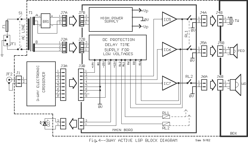
In the Fig.4,
appear a big part of various stages and connections between them. As it appears the
speakers are placed in suitable wooden box. In his rear part of box and on a leaf of
aluminum are placed the power transformer T1, the power bridge rectifier BR1, the switch
S1, the main power plug JF1, fuse F1, the RCA plug JF2 and the indicative led D27.
Transformer T1 has two outputs A=2X38Volts and B=2X15Volts.
Bridge BR1 clinching above in aluminum so that it�s frozen. On a big heatsink clinching
the IC5-6-7. In plug JF2 enter the acoustic low level signal from the preamplifier exit.
Good it�s the crossover PCB it�s found far by the T1 transformer.
|
| T1=110-230Vac||A=2X38V
>350VA |
JF2=Female RCA Jack |
MID=MIDRANGE 8 ohms |
|
B=2X15V 30VA |
F1=FUSE 1.2A SLOW+CASE |
WOO=WOOFER 8ohms |
| BR1=BRIDGE RECTIFIER 400V
35A |
S1=2XON-OFF 15A Switch |
|
| JF1=3pin male supply jack |
TW=TWEETER 8R |
|
|

Fig.5--Crossover
calculation |
|
|
|
|
|
|
|
Sam
Electronic Circuits 9/02 |
|
|
