����
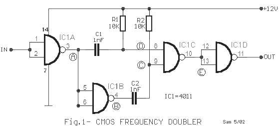
�� ������� ����� ���� ������������ ����������
������������ ��� �������� CMOS, ��� ������� NAND,
����� 4011. �
������������ ���������� ����������� ��� ����
���������� IC1B, ��� ����������� ��������������
��� �� R1/C1, R2/C2 ��� ��� NAND ����� IC1A, IC1C ��� IC1D ���
����������� ��� ���������� ������� ��� ������.
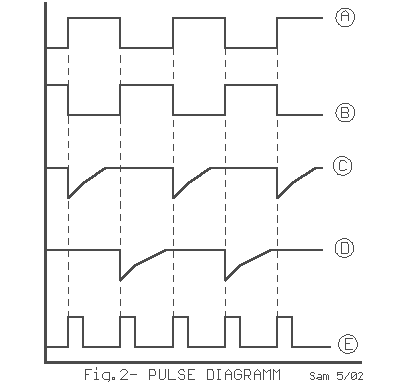
��� Fig.2 , �������� �� ������ �� ������� ������ ���
����������
This frequency doubler uses one CMOS quad, two input NAND
gate package type 4011. The
frequency doubler proper consists of an inverter IC1B, two differentiating networks R1/C1,
R2/C2 and NAND gate IC1A, IC1C and IC1D function as input and output buffers. In Fig.2
exist the pulses in different points of circuit. |