�����
� ������������ ���������� ������������ ���
������������ ������� hex inverter 4069.
���� ������������ ���������� ������ ��
������������� ��� �� ����� ��� ����� ������
������, ��� ������ � ��������� ����� ��� �����
���� ��� ������������ ������� �������. �� ����
����������� ���� ������ ��� N1. ������ �� �����
��� ���������� �� duty-cycle ������� 50%, �� �������
������� �� �� ������ CMOS, (3- 15V ��� ������ �� ������
������� �� ��� ���� �����������). �� ���� �������
������������ ��� ������������ ��� N1, ���
������������ ���� ��� �� �2, ���� �� ����������
��� ������ � ��� � ��� N1 ��� ��� �2 �����
���������� �� ������� ����� 180� . �
������ N1, ������������ ��� �� C1 ��� R1 ��� � ������
��� �2 ������������ ��� �� C2 ��� R2, ��� ������
����������� �� ��� ������ ��� ������ C ��� ��� D,
�� ������� ����� 180� . �� ������
�������������, ������������� ��� ��������������
��� ��� N3 ��� N4. ���� ������������ �� ��� NOR ����
��� ����������� ��� �� D1, D2, R3 ��� N5, ���
������������� ������ ��� ��� N6 ��� �� ������ ���
�����, ��������� ��� ����� ���� ��� �������
�������. �� ������� �� ������������ ��� ��� ����
����� ����������. �� ��� ����� ��� ������������
��� ��� ����� ������ ��� ������ E ��� F 500ns, �� duty
cycle ���� ����� ��
����� 50%, ����� � ��������� ����� 1MHZ, ���� �
��������� ������� ����� 500KHZ.
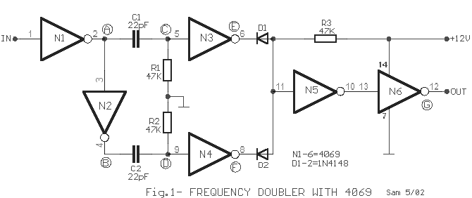
This frequency doubler using a single 4069 hex inverter IC, a frequency
doubler can be constructed to give an output pulse train whose frequency is twice that of
a squarewave input signal. The signal is applied to the input of N1. It should be a
squarewave with a duty-cycle of approximately 50% at level compatible with CMOS logic
(3-15V peak to peak depending on supply voltage). The input signal is buffered and
inverted by N1, and inverted again by N2, so the outputs A and B of N1 and N2 are
squarewave signals 180� out of phase. The output of N1, is
differentiated by C1 and R1 and the output of N2 is differentiated by C2 and R2, giving
two spike waveforms of C and D, 180� out of phase. The signals
are buffered, inverted and shaped by N3 and N4. These are then combined in a NOR gate
consisting of D1, D2, R3 and N5, and finally inverted by N6 to give the frequency twice
that of the input signal. The circuit will operate over a wide frequency range. With the
component values shown the width of pulses in E and F point is about 500ns, so the duty
cycle of the output will be 50% when the frequency is 1MHZ, when the input frequency is
500KHZ.By A.M. Bosschaert |