LOGIC OPERATOR
AND Gate
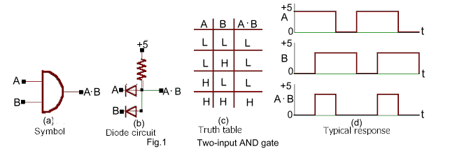
� ���� AND ���� ��� �������� ��� ��� ����� ��� ����� �H�, �� ��� �� ��� ������� ����� �H�. � ��������� ��� ����� AND �����: Y=A�B ��� � ������� �������� ��� ����� AND ������������� ���� Fig.1c .
The symbol for an AND gate is shown in Fig.1a where A . B is read "A AND B". As indicated in the truth table, an output appears only when there are inputs at A AND B. If the inputs are in the form of positive voltage pulses [with respect to ground], inputs at A and B reverse bias both diodes, no current flows through the resistance and there is a positive output (H).In general, there may be several inputs terminals. If any one of the inputs is zero (0) current flows through that forward-biased diode and the output is nearly zero (0). For two inputs varying with time , a typical response is sown in Fig.1d.
OR Gate
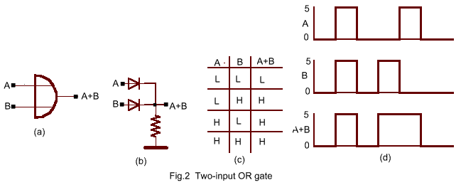
� ���� OR ���� ��� �������� ��� ��� ����� ��� ����� �H�, �� ����������� ��� ��� ��� ��� �������� ����� �H�. � ��������� ��� ����� OR �����: Y=A+B ��� � ������� �������� ��� ����� OR ������������� ��� Fig.2c
The symbol for an gate is Fig. 2a where A+B is read "A OR B". As indicated in the truth table , the output is (H) if input A OR B is (H). For no input (zero voltage) in Fig. 2b, no current flows and the output is zero (0) .An input of +5 V (H) at either terminal A or B or both (or at any terminal in the general case) forward biases the corresponding diode , current flows through the resistance and the output voltage rises to nearly 5V (H). For two inputs varying with time ,the response is as shown.
NOR Gate
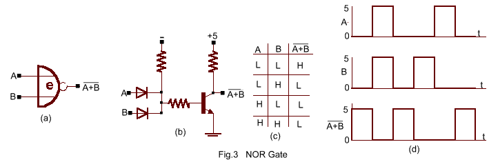
In the diode OR gate Fig.3b ,a positive input at A OR B produces a voltage
across R and a positive output voltage . But this output is less than the input (by the
diode voltage drop) and after a few cascaded operations the signal would decrease below a
dependable level. A transistor can be used to restore the level Fig.3b however ,the
inherent inversion results in a NOT OR or NOR operation. The small circle on the NOR
element symbol and the bar in the ![]() output indicate the inversion process. In the Nor
circuits with no input no input , the transistor switch is held OFF by the negative base
voltage and the output is +5V (H) .A positive voltage at terminal A or B raises the base
potential, forward biases the emitter
output indicate the inversion process. In the Nor
circuits with no input no input , the transistor switch is held OFF by the negative base
voltage and the output is +5V (H) .A positive voltage at terminal A or B raises the base
potential, forward biases the emitter
junction , turns the transistor switch ON and drops the output to nearly zero (0). In addition to restoring the signal level, the transistor provides a relatively low outputs impedance so that this NOR element can supply inputs to many other gates . Another advantage is that all the basic operations can be achieved using only NOR gates.
NAND Gate
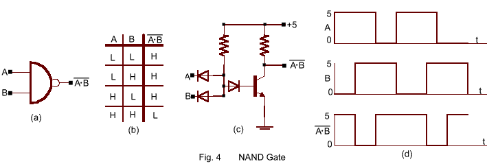
Diodes and a transistor can be combined to perform an inverted AND function.
Such a NAND gate has all the advantages of a NOR gate and is very easy to fabricate ,
particularly in integrated circuit form. In a complex logic system it is convenient to use
just one type of gate , even when simpler types would be satisfactory , so that gate
characteristics are the same throughout the system. The NAND gate function is defined by
the truth table in Fig. 4 .The small circle on the NAND element symbol and the bar on the ![]() output
indicate the inversion process. With positive inputs at A and B (H AND H ) ,the diodes are
reverse biased and no diode current flows ; the positive base current causes heavy
collector current and output is approximately zero (0). If either A or B has a zero (0)
input , at least one diode conducts to ground , the emitter junction voltage drops below
the critical value ,no base current and hence no collector current flows, and the output
is +5V (H). For more positive cutoff, a second diode may be placed in series with the base
of the transistor.
output
indicate the inversion process. With positive inputs at A and B (H AND H ) ,the diodes are
reverse biased and no diode current flows ; the positive base current causes heavy
collector current and output is approximately zero (0). If either A or B has a zero (0)
input , at least one diode conducts to ground , the emitter junction voltage drops below
the critical value ,no base current and hence no collector current flows, and the output
is +5V (H). For more positive cutoff, a second diode may be placed in series with the base
of the transistor.
NOT Gate
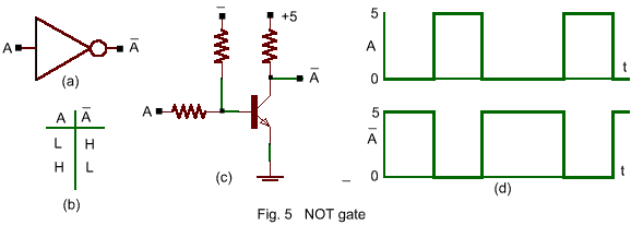
The inversion inherent in a transistor circuit corresponds to a logic NOT
represented by the symbol in Fig. 5 where ![]() "NOT A ". As indicated in the truth table, the
NOT element is an inverter the output is the complement of the single input. With no input
(0) the transistor switch is held open by the negative base voltage and the output is +5V
(H). A positive input voltage (H) forward biases the emitter junction, collector current
flows, and the output voltage drops to a few tenths of a volt (0). For a changing input,
the output response is as shown.
"NOT A ". As indicated in the truth table, the
NOT element is an inverter the output is the complement of the single input. With no input
(0) the transistor switch is held open by the negative base voltage and the output is +5V
(H). A positive input voltage (H) forward biases the emitter junction, collector current
flows, and the output voltage drops to a few tenths of a volt (0). For a changing input,
the output response is as shown.