| E���� ������ ���
�� ��������� CMOS ������������ ���� ������
��������� �������, ���� ��� ���� ��� ���
��������� ���� ������� ��� ����� �����, ��
������������ ��� ������ ��������� ����� ������ ,
��� ����� �������� �� ��������������� ���������
���� �� ���������� ������� ���������. �� ���� ���
���� ���������� ��� � ���������� ��� ��������
������ . ��� ������� �������� �������� ����� NAND
��� ��� J-K FLIP FLOP. � ���� U1 ����� ����������������
��� ��������� ����� ��� �� ����� ��� Schmitt trigger.
���� ��������� ������� ������ ������ [0] ����
������ ��� U1 ,���� ��� R2 ��� ���� ����� ��� [1], ��
���������� �� ��� ���� � ������ D1. ����������
���� ������ U2 ,������� ������ [1], ���� ��� R4. ����
����� ���� ������ [0], �� ���������� � ������ ��� U3
�� ���� ������ [1] ��� � ������ ��� U4 �� ���������
��� ������ [0].���� ������������ �� ������� ���
���� ����� � (��������� � ��������� ���������
���������, ��� ��� ������ �� ����������� ������),
���� ������ ��� U1 ����������� ��� ���� 50��, ���
���������� ��� �� ���������� ��� ������������ ��
����������� �������, �� ��������� �����������
��� ������ ,������ ������� ��� ����� D1, �����
������� �� ���������� � �������� C4, ���� ��� ���
��������� R4. ���� ��� ���� ������ ���
������������� (��� �� ��� �������� �������
���������� ��� �������� ), ����������� ����
������ ��� U2 ��� ���� �������� ������ ��� ����
����� ��� U4, ��� ������� ������ ������, ��
���������� �� ������� ��� ��������� ��� IC2. ��� ��
��������� ��� ���������� ��� ���������� , ���� ��
������ �� ��������� � R2.����� ������������� ��
������� ��� ��� ��� ����� , ������������ ��
������ 50 �� ���� ������ ��� U1, ����������� � D1,
������������ � C4 ���� ��� ��� R3 ��� �����������
������ [0] ���� ����� ��� U4, � ��������� ��� J-K flip-flop
���� ��� ������� ���� ��� ���� ���������. ��� ��
������� � ��������� ��� J-K flip-flop ������ ��
������������ ���� ��� ����� � . ��� ��� �������
��� IC2, �������� �� ���������� ������� ���������
������ , ����������� ��' ���� ��� �� ������ ��� IC2,
����� ��������������� (���� � ��� ����� [1]����
��������� 1, � ���� ����� [0],���� ��������� 2). ��
������� ������ �� �R1 ��� ��� ���� RL1, ���� ������
�� �������� ��� TRIAC , ���� ���� optocoupler �
����������� ���� ������� ,����� ��
���������������� ��� ��������� ����������. ���
��� �������������� �� ������� flip-flop ��� IC 2 ,����
�� ������� ������ �� �������� . �� ������� ������
�� ������������ �� ���� ��������������� ��� 6-15V
��� �� ����� ������� 1ma ,����� ��� ���������� ���
������.
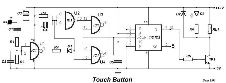
Is acquaintance that circuits CMOS
present very big resistance of entry, thus if through this resistance it passes a small
current, will be created a enough important fall of voltage, which we can exploit suitably
so that we drive various circuits. In this beginning is supported also the operation of
touch switch. In the circuit exist four gates NAND and a j-k FLIP FLOP. The Gate U1 is
connect, as voltage amplifier and the other as schmitt trigger. In the situation of calm
we have logic [ 0 ] in the entry of U1, via the R2 and in the his exit [ 1 ], so that not
conduct the D1. Simultaneously in entry U2, exists logic [ 1 ], via the R4. In the exit it
has logic [ 0 ], with result the exit of U3 has logic [ 1 ] and the exit of U4 it finds in
the logic [ 0 ]. . When we touch the finger our in contact T (square or round metal
surface, that should not oxidise easily), in the entry of U1 is applied a signal 50HZ,
that come from the environment and is changed in square pulses, the negative half-s period
of which, make conductible the D1, whenever it begins charge the capacitor C4, through
resistance R4. After few tenths of second (in order to do not exist accidental excitations
from noises), it is presented in the entry of U2 a slow negative forehead and in the exit
of U4, a abrupt positive forehead, so that it changes the situation of IC2. In order to we
increase the sensitivity of circuit, then it will be supposed is decreased the R2. Hardly
we remove the our finger from the contact, they are suppressed the pulses 50 HZ in the
entry of U1, it is cut-off the D1, discharge the C4 through the R3 and comes back in logic
[ 0 ] in the exit of U4, the situation of j-k flip-flop however it does not change because
has locked. In order to changes the situation of j-k flip-flop it should we touch again
the contact T. From the exits of IC2, we can drive various circuits of power, taking into
consideration that the exits of IC2, are complemental (when the one is [1] in pin 1, the
other is [ 0], in the pin 2. The circuit drive the TR1 and relay RL1, but can drive a
TRIAC, via a optocoupler or any other circuit, it is enough we use the suitable
adaptation. If is not used the second flip-flop of IC 2, all the entries it should in 0V.
The circuit can be supplied with stabilised voltage from 6-15V DC and the current roughly
1ma, except circuit that drives.
|