|
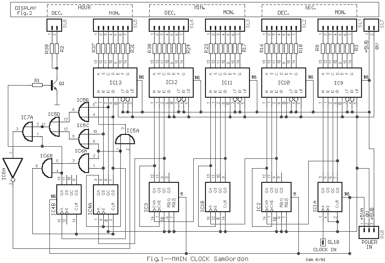
1. Main Clock
|
With
pleasure the lot of friends of digital clocks that use discernible components, will see
this circuit. It's a clock, with 12hour clue, little simpler in the manufacture from the SamClock. It�s a
designing that became from the friend George Kordogiannis in 1990, which was modified and
corrected in enough points by my, until it reach in the current form. Most completed that
uses is TTL, apart from the IC9 until IC13, that is CMOS, that they have the faculty to
drive display Common Cathode. In the place of 4511 [6], can be placed the
74LS47 [7],
which can drive display Common Anode. In this case it will be supposed they are changed
display Common Cathode in the Fig.2, with Common Anode, changing of course and connection
in DIS1 until DIS5 display. In the SL10, come in the pulses frequ. 1HZ [fig.3-4], which then
are divided successively by the IC2 until IC4 and the round this gates, ensuring the clue
of time, in Hours, Minutes and Seconds. The Q1 drive display the tens of hours [Fig.2],
but only the B and C Led of DIS6 display [Fig.2], ensuring clue 1, when needs the clue of
hours it�s 10, 11, 12. The voltages that supply the circuit are divided in two lines.
The voltage +5VA supplies all IC except the IC9 until IC13 and is supplied with voltage in
case of break of network voltage, on the contrary the voltage of +5VB, supplies only the
IC9 until IC13 and display and is interrupted in case of interruption of network voltage,
ensuring thus economy in battery [Fig.5]. If the Q1 is hot, can be placed on a small
heatsink
|
| R1=2.2Kohm 1/4W
5% |
IC5-7=74HC32
[3] |
Q1=BD139 on Heatsink |
| R2......R38=470ohm
1/4W 5% |
IC6=74HC08
[4] |
SL1....SL5=7 pin connector |
| IC1-4=74HC390 [1] |
IC8=74HC04
[5] |
SL6-7=2 pin connector |
| IC2-3=74HC92 [2] |
IC9....IC13=4511 [6]
or [74LS47] [7] |
SL8=3 pin connector |
|
| [1]
74HC390 or 74LS390= Dual 4bit Decade and Binary COUNTER |
[5]
74HC04 or 74LS04= Hex inverter |
| [2]
74HC92 or 74LS92= Decade, divide by 12 and Binary COUNTER |
[6]
4511= BCD to 7-segment Latch/Decoder/Driver for CC Display* |
| [3]
74HC32 or 74LS32= Quad 2-input OR gate |
[7] 74LS47=
BCD to 7-segment Decoder/Driver for CA Display* |
| [4]
74HC08 or 74LS08= Quad 2-input AND gate |
CC=Common
Cathode |
CA=Common
Anode |
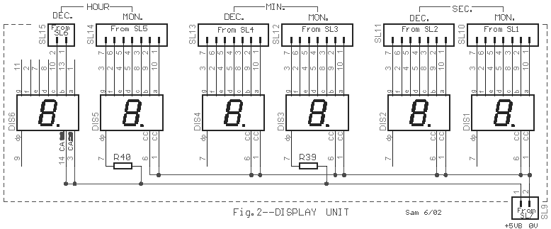
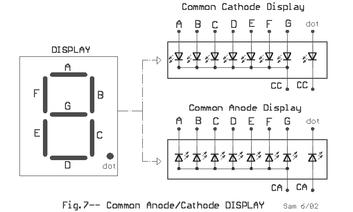
2. Display
In the
Fig.2, exist the clue display. As he is drawn, the drive of display becomes when in the
place of IC9�.IC13, are used the 4511 [6]. Thus DIS1 until DIS5,
are Common Cathode and DIS6 of it�s in every case Common Anode. If are
used the 74LS47 [7], then the DIS1�DIS5 it should they are changed
with Common Anode, the pins 1 and 6 of DIS1 until DIS5, they go to the line of + 5VB and
the R39-40, in the line of 0V. The R39-40, turn on the dot in the DIS3 and DIS5, so that
exist a divide the displays that shows the Hours, Minutes and Seconds.
|
| R39-40=220ohm
1/2W 5% |
DIS6=20 mm Led Display Common
Anode |
SL10.....SL4=7 pin connector |
| DIS1-5=20 mm Led Display
Common Cathode* |
SL9-15=2 pin connector |
*See Text |
|
| *DIS1-5=20 mm Led Display
Common Cathode with driver 4511 [6] |
*DIS1-5=20 mm Led Display
Common Cathode with driver 74LS47 [7] |
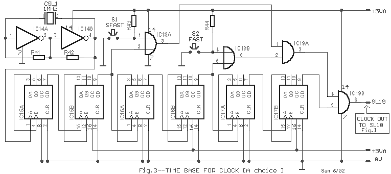
3. Time Base [A Choise]
|
For the
production of pulses 1HZ that constitutes also the base of time for the clock exist two
proposals. And the two are based on the same beginning of operation. A oscillator with
crystal in high oscillation frequency and then division of this frequency so that we take
in the end the frequency 1HZ. This process us ensure very big precision and stability in
the produced pulses. The oscillator in the Fig.3 is based on a crystal in frequency 1MHZ
and then in frequency division of 1MHZ in stages via 10, from the IC15 until IC17. The gates
IC18A-B until IC19A-B do not participate immediately in the operation, only that
indirectly when are pressed the switches S1 or S2, which us allow the regulation of time.
Pressing S1 [Super Fast] and S2 [Fast], are released pulses of frequency 10KHZ and 100HZ
respectively, making the clue in display run very fast facilitating in the regulation of
TIME, in short time interval. The supply of circuit becomes from the line + 5VA, ensuring
thus the operation of oscillator, even in interruption of network voltage, supplied from
the battery.
|
| R41-42=470ohm |
IC14=74HC04* |
IC19=74HC08* |
| R43-44=10Kohm |
IC15-16-17=74HC390* |
S1-2=Push Button normal open |
| CSL1=1MHZ Crystal |
IC18=74HC32* |
*See component list in Main
Clock |
|
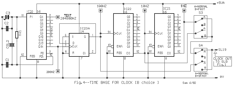
4. Time Base [B Choise]
In the
Fig.4, exist a proposal that is based on the same beginning of operation as on the Fig.3,
but exist a crystal with higher operation frequency 3.2768MHz, with successive division,
in order that in the end we take frequency 1HZ, in exit SL19. With variable capacitor C3
we can regulate thus the oscillator in order that in point TEST we take pulses of
frequency 204800HZ. With switches S1 [Fast] and S2 [Super Fast] we regulate the display
clue in process of regulation, with frequency 10HZ and 100HZ, respectively, making the
clue in display to run very fast, facilitating in the regulation of time in short time
interval. The supply of circuit becomes from the line + 5VA, ensuring thus the operation
of oscillator, even in interruption of network voltage, supplied from the battery. The
solution of mechanic switches, was preferred for simplicity reasons.
|
| R45=10Mohm |
IC20=4060
[8] |
CSL2=3.2768 MHZ crystal |
| C1-2=22pF ceramic |
IC21-22=4017 [9] |
S3-4=Push switch recrudescent |
| C3=22pF trimmed capacitor |
IC23=4013
[10] |
|
|
| [8]
4060=14-stage Ripple Carry Binary Counter/Divider and Oscillator |
[10]
4013=dual D Flip-Flop |
| [9]
4017=Hex "D"-type Flip-Flop |
|
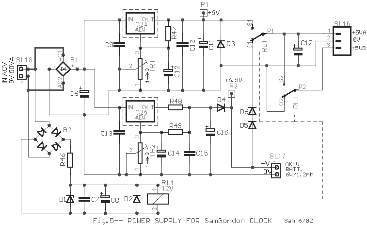
5. Power Supply for SamGordon
Clock
|
In the
Fig.5, exist the power supply that gives essential voltages for the operation of circuit,
the battery charge and the transfer in the battery when exist interruption of network
supply. The regulated from the TR1, voltage regulator IC24 is regulated so that it gives
in his output + 5V [P1]. With this voltage function the circuit. Second regulator IC25, is
regulated by the TR2, so that it gives in point [P2] voltage + 6.9V, with which becomes
the battery charge of lead acid 6V/1Ah, which is connected in the SL17. In the case of
interruption of network supply then turn off very fast the RL1 and his contacts goes to
the place that is drawn in the Fig.5. The voltage line + 5VA is connected via the D5-6 in
battery 6V, on the contrary the line + 5VB is led to the 0V and the Display stops they
show. The remainder parts of circuit working continue and they measure the time, until
changes the situation therefore display will work once again showing regularly the time.
In the duration of contacts transfer from a situation in other the supply of circuit
becomes from the C17. The IC24-25 should be placed on a good Heatsink and the regulations
the TR1-2 he becomes without are connected the circuit in the supply output and the
battery it is except.
|
| R46=1.2Kohm 2W |
C16=1uF 25V |
B2=4 X 1N4001 |
| R47-49=270ohm |
C17=1000uF 16V |
RL1=12VDC 2X2 [10A] |
| R48= |
D1=12V 1W zener |
TR1-2=4.7Kohm
trimmer |
| C6=2200uF 25V |
D2-3=1N4002 |
SL17-18=2 pin connector |
| C7-9-10-13-15=100nF 100V MKT |
D4-5-6=1N5408 |
SL16=3 pin connector |
| C8-12-14=10uF 25V |
IC24-25=LM317 on
Heatsink |
BATT=AKKU battery 6V/1.2Ah |
| C11=47uF 25V |
B1=100V 3A Bridge Rectifier |
|
|
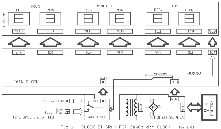
6. Block Diagram
7. Connection for
Display common Anode or Cathode
|
In the
Fig.6, exist the Block diagram of basic connections between the various inputs and
outputs. In the Fig.7, exist the connectin for Display Common Anode and Common Cathode.
Soon, as I will find time I will draw also the printed circuit, which I will also give. In those that
him will make, I wish good success. |
Sam
Electronic Circuits 6/02 |
|
|